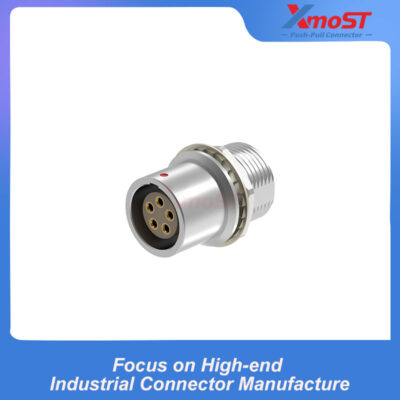
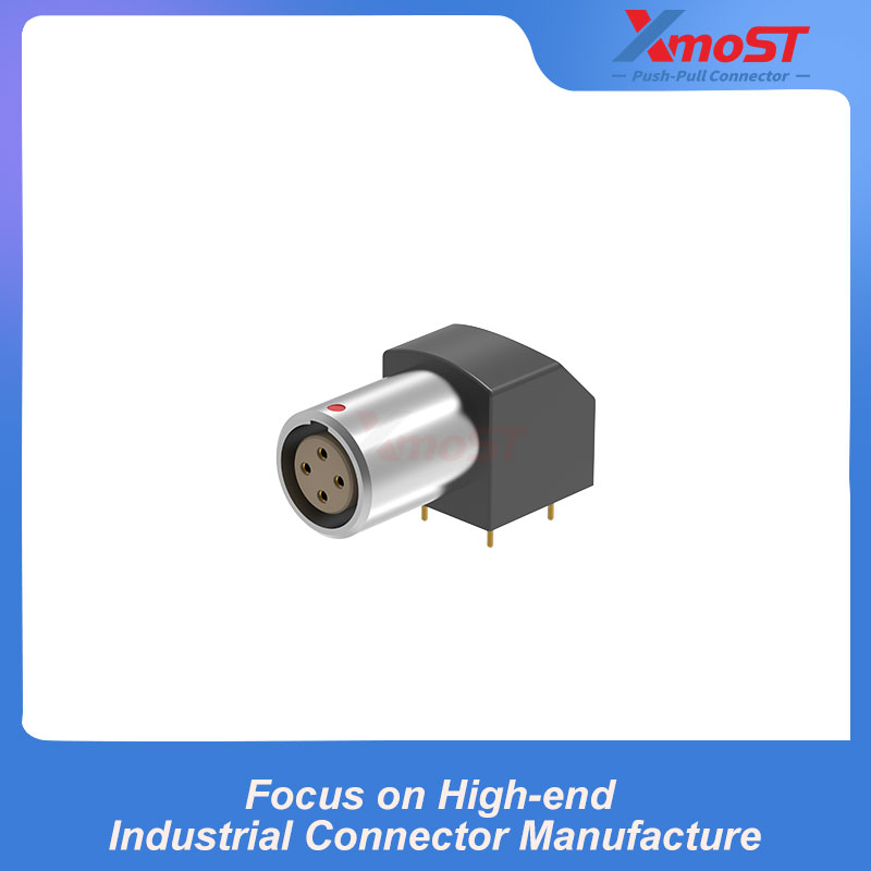
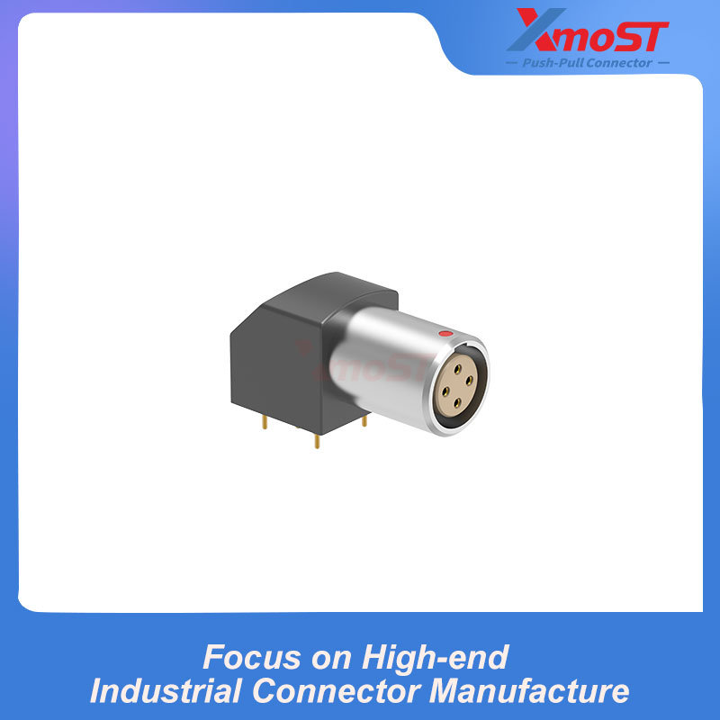
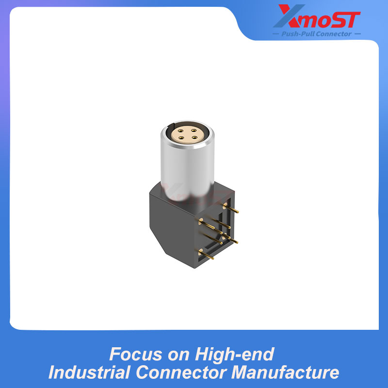
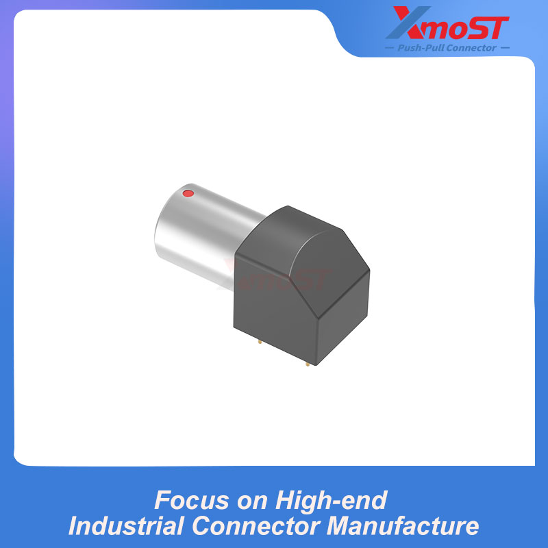
XM-LEPG is a B Series right-angle female receptacle designed for direct installation on a printed circuit board. Its 90° PCB terminals allow the mating direction to remain parallel to the PCB, making it suitable for equipment with limited internal height or side-entry connector requirements.
Connector incorporates solderable grounding tabs that provide an electrical grounding path and help secure the connector assembly to the PCB. Its female mating interface is compatible with corresponding B Series Push-Pull male plugs for fast, secure and tool-free connection.
A standard G key ensures correct connector orientation. Optional A–M key configurations are available to help prevent cross-mating between similar connectors used in the same system.
Product Features
- Right-angle female receptacle for direct PCB mounting
- 90° through-hole PCB terminals
- Solderable grounding tabs for grounding and board retention
- Compatible with the B Series Push-Pull self-latching system
- Fast, secure and tool-free mating
- Standard G key for correct connector alignment
- Optional A–M key configurations
- Available in 00, 0B and 1B sizes
- Multiple contact configurations available
- Space-saving design for side-entry PCB connections
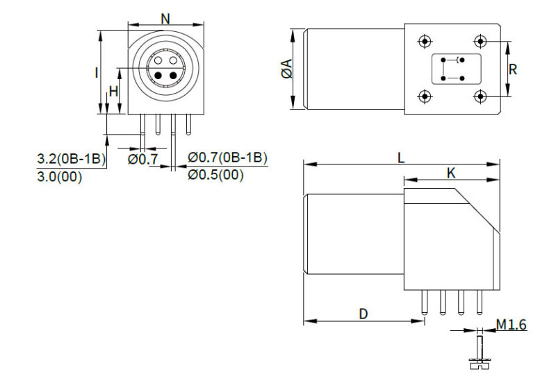
Dimensions
All dimensions are in millimetres.
| Size | A | D | H | I | K | L | N | R |
| XM-LEPG.00.302.HLN XM-LEPG.00.303.HLN XM-LEPG.00.304.HLN |
6.8 | 11.5 | 3.5 | 7.0 | 8.7 | 19 | 7.1 | 5.08 |
| XM-LEPG.0B.302.HLN XM-LEPG.0B.303.HLN XM-LEPG.0B.304.HLN XM-LEPG.0B.305.HLN XM-LEPG.0B.306.HLN XM-LEPG.0B.307.HLN XM-LEPG.0B.309.HLN |
9 | 14.6 | 6.7 | 12.7 | 13.3 | 25 | 11.7 | 7.62 |
| XM-LEPG.1B.302.HLN XM-LEPG.1B.303.HLN XM-LEPG.1B.304.HLN XM-LEPG.1B.305.HLN XM-LEPG.1B.306.HLN XM-LEPG.1B.307.HLN XM-LEPG.1B.308.HLN XM-LEPG.1B.310.HLN |
11 | 16.6 | 7.5 | 14 | 13.3 | 27 | 12.6 | 7.62 |
PCB Terminal Reference
| Size | PCB Terminal Length |
| 00 | 3.0 mm |
| 0B–1B | 3.2 mm |
Drawing indicates terminal diameters of Ø0.5 mm for size 00 and Ø0.7 mm for sizes 0B–1B. The grounding and fixing terminal dimensions should be checked against the corresponding PCB drawing before footprint design.
Typical Applications
- Industrial control electronics
- Test and measurement instruments
- Medical and laboratory devices
- Communication equipment
- Embedded control systems
- Compact PCB assemblies
- Automation and robotic equipment
- Side-entry equipment interfaces
Solder-side and mating-side contact correspondence varies by contact configuration. Confirm the official PCB footprint and contact-arrangement drawing before completing the PCB layout or placing an order.